Search The World

Custom Search
sponsors
What type of antenna used in the mobile?
Answer is Omni directional antenna used in the mobile. There are various types of antenna used in mobile like, PIFA (Polar Inverted F Antenna) FICA etc
Radar Equation
The power Pr returning to the receiving antenna is given by the radar equation:
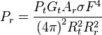
where
- Pt = transmitter power
- Gt = gain of the transmitting antenna
- Ar = effective aperture (area) of the receiving antenna
- σ = radar cross section, or scattering coefficient, of the target
- F = pattern propagation factor
- Rt = distance from the transmitter to the target
- Rr = distance from the target to the receiver.
In the common case where the transmitter and the receiver are at the same location, Rt = Rr and the term Rt² Rr² can be replaced by R4, where R is the range. This yields:
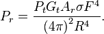
This shows that the received power declines as the fourth power of the range, which means that the reflected power from distant targets is very, very small.
The equation above with F = 1 is a simplification for vacuum without interference. The propagation factor accounts for the effects of multipath and shadowing and depends on the details of the environment. In a real-world situation, pathloss effects should also be considered.
sponsored by
Wednesday, July 29, 2009
Sunday, July 19, 2009
DELTA MODULATION
AIM:To study the delta modulation process by comparing the present signal with the previous signal of the given modulating signal.
APPARATUS:1. Delta modulation trainer kit
2..Dual trace CRO
3.Digital multi meter
4.CRO probes and set of patch cards
THEORY:Delta modulation is a differential PCM technique in witch the difference signal between two successive samples is encoded into a single bit code . The process of encoding is as follows .The comparator compares the in put signal m(t) and r(t) .
If m(t) >r(t) logic 1 is generated at the out put of the comparator. Otherwise a logic 0 is generated. the value of logic 1 or logic 0 is termed as ∆(t) is held for the bit duration by the sample and hold current to generate So(t) , the delta modulated out put .
This out put So(t) is fed to the 8bit binary up/down counter to control its count direction . A logic’1’ at the mode control in put increases the count value by one And a logic ‘0’ decrements the count value by one . All the eight out puts of the counter are given to DAC to reconstruct the original signal .In essence the counter and decoder forms the delta modulation in the feed back loop of the comparator .Thus if the input signal is higher then the reconstructed signal the counter increments at each step so as to enable the DAC out put to reach to the input signal values.Similarly the in put signal m(t) is lower then the reconstructed signal r(t) , the counter decrements at each step and the DAC output gets reduced to reach a value m(t) .
PROCEDURE:1.Verify the circuit as per circuit diagram .
2. connect clock signal to the delta modulator .
3. Connect modulating signal to the input of delta modulator and observe the same on channel one .
4.Observe the delta modulation out put on channel 2.
5.Connect this delta modulator out put to the demodulator.
6.Also connect the clock signal to de modulator .
7.Observe the de modulator out put with and without RC filter on CRO.
PRECAUTIONS:
RESULT:
VIVA VOICE:1.What is the aim of the experiment?
2.What is delta modulation ?
3. What is demodulation ?
4. Why we need modulation ?
5. What is the use of modulation ?
Standard Text Books For JNTU ECE Students
1 Electronics Devices and Circuits U.A.Bakshi A.P.Godse Technical Publications
2 Linear Integrated Circuits D.Roy
3. Op-amps And Linear IC’s Ramakanth.A.Gayakwad
4. Operational Amplifiers and Linear Integrated Ckts R.F.Coughlin and Fredrick Driscall
5 Linear IC Applications U.A.Bakshi A.P.Godse Technical Publications
6. Design With Op-amps &Analog Integrated Circuits sergio Franco
7 Digital Design M.MorrisMano Pearson Publications
8. Digital Logic Design A.P.Godse D.A.Godse Technical Publications
9 Pulse And digital Circuits A.Anand Kumar PHI
10 Pulse And digital Circuits J.Milman and H.Taub McGrawHill
11 Signals & Systems B.P.Lathi BSPublications
12 Signals & Systems Simon Haykins
13 Mechatronics W.Boltan Pearson Education 3rdedition
14 Manuals On Mechatronics —– Cyber Motion Technologies
15 Digital Signal Processors VenkataRamani And Bhaskar Tata McGrawHill
16 Antenna Theory C.A.Balanis John WileyEdu
17 Digital Signal Processing P. RameshBabu Scitech Publications
18 Digital System Design by using VHDL Roth Thomsan India Limited
19 Integrated Electronics Milman And Halkias Tata McGrawHill
20 Electronic Devices and Circuit Theory Boylested Pearson Education
21 Digital Communications Simon Haykins Wiley India Pvt
22 Principles Of communication Systems H.Taub and D.Schiling TMH
23 Communication systems Analog & Digital Singh & Sapre Thomsan India Ltd
24 Modern Analog &Digital Communication B.P.Lathi Oxford reprint 3rdedition,2004
25 Digital & Analog Communication Systems K.Samshanmugam Wiley India PVT
26 Electronic CirCuit Analysis A.P.Godse U.A.Bakshi Technical Publications
27 Electronic CirCuit Analysis K.Lalkishore BSPublications
28 Micro Electronic Circuits Analysis & Design M.H.Rashid Thomsan PWS
29 Optical Fiber Communications Gerd Kaiser(3rd&4thedition) McGrawHill
30 Optical Fiber Communications John.M.Senior PHI
31 Introduction to Radar Systems Skolnik(2nd edition) McGrawHill
32 Introduction to Neural Networks using MATLABS.N. ShivanandamS.N.DeepaS.Sumathi TMH
33 Elements of Artificial Neural Networks KishanMehrotraChelukuri.k.mohanSanjay ranka Pearson Publications
34 Introduction to Artificial Neural Systems J.M.Zurada(3rdedition) Jaico Publishers
35 Electronic Instrumentation(2ndedition) H.S.Kalsi
36 Measuring Systems, Applications&Design E.O.Doeblin(4thedition) McGrawHill
37 Electronic Measurements&Instrumentation K.LalKishore Pearson education
38 Principles of Electrical& Electronic Engineering V.K.Mehta S.Chand&Co
39 Digital Image Processing R.C.Gonzalez&R.E.Woods Pearson publications
40 Fundamentals Of Digital Image Processing A.K.Jain PHI
41 Digital Image Processing using MATLAB R.C.Gonzalez&R.E.Woods Pearson education
42 Digital Image Processing William.K.Pratt(3rdedition) JohnWiley
43 Fundamentals of Electronic Image Processing WeeksJr Spic/IEEESeriesPHI
44 Probability, Random Variables &Random signal Processing Z.Peebles(4thedition)TMH
45 Probabilty, Random Variables&Stochastic Processes AthanasiosPapoulis(4thedition PHI
46 Probabilty,statistics and RandomrocessesP.Guruswamy&K.MurugesonAnuradhaPublishers
47 Stastical Theory of Communication S.P.Engine Xavier New Age Publications
48 Probabilty theory of &stochastic Processand its applications T.VeeraRajan
Radar Systems Question Papers
UNIT I
1. Draw the block diagram of a Pulsed radar and explain its operation
2. Write the relative factors between the radar’s cross section of the target and its true cross sections
3. Derive basic radar’s equation
4. Explain about the frequencies used for radar
5. Discuss in detail the choice of various parameters that are affecting the radar range
6. Derive the range equation and discuss about its limitations
7. what do you understand by false alarm
8. A pulsed radar operating at 10GHz has an antenna with a gain of 28dB and a transmitter power of 2KW . If it is defined to detect a target with a cross section of 12sq.m and the minimum detectable signal is Pmin= -90dBm. What is the maximum range of the radar
UNIT II
1. What is meant by minimum detectable signal in radar. Discuss the effects of integration of radar pulses
2. What are the desirable pulse characteristics and the factors that govern them in a radar system
3. Discuss about detection of signals in noise
4. Describe the different noise components present in radar systems
5. Explain about PRF and range ambiguities
6. Explain about radar cross section of targets
UNIT III
1. Explain about Doppler effect
2. Explain the operation of CW radar with neat block diagram
3. derive the expression for the velocity of the target when the target is moving away from the radar in the case FM-CW radar
4. an 8GHZ Police radar measures a Doppler frequency of 1788HZ from a car approaching the stationary police vehicle in an 80 km/h speed limit zone .what should the police officer do?
5. Differentiate the operation of pulse radar from simple CW radar
6. Draw the block diagram of non coherent MTI radar and explain the function of each block in detail
7. Explain the advantages of non coherent MTI Radar
8. Explain the applications of CW radar.
9. Explain the principle of Doppler effect and its application CW radar.
10. Derive an expression for unambiguous range of a two frequency CW radar.
UNIT IV
1) Explain the principle of operation FM –CW altimeter with suitable diagrams.
2) Determine the beat frequency due to range and the quantization error if range=100m, and the frequency excursion is 75Hz and modulating frequency is 1Khz.
3) Explain the operation of sideband superhetreodyne CW Doppler radar with block diagram.
4) Explain how the noise signals are limiting the performance of FM-altimeter .
5) What are advantages and disadvantages of FM-CW radar over multiple frequency CW radar.
UNIT V
1) A simple MTI delay line canceller is an example of time domain filter .Why? Explain.
2) Enumerate the advantage of the time delay line canceller as compared to the convention frequency domain filter.
3) Draw the bloc diagram of four pulse canceller and find the weight for the same.
4) Differentiate three- pulse canceller from four pulse canceller.
5) Description of Range gate Doppler filters.
6) Differentiate blind phases from blind speeds.
7) Explain the effect of Doppler frequency ‘fd’ for the stationary objects and moving targets.
8)Explain the butterfly effect that is produced by MTI.
9) Draw and explain frequency response characteristics of a MTI using range gates and filters.
10) How does MTI radar differ from CW radar?
11) How does MTI radar differ from pulse Doppler radar?
12. What is the distinctive feature that makes the MTI radar and Pulse Doppler to differ ?
UNIT VI
1) Explain Tracking Principles
2) Explain the block diagram of amplitude comparison monopulse radar for single angular coordinate and explain its operation
3).Explain phase comparison monopulse tracking radar technique
4).Explain the block diagram of AGC portion of tracking radar receiver
5).Explain about sequential Lobing
6).What are the advantages of monopulse radar over conical scan radar?
7).Distinguish between search radar and tracking radar?
8).Compare the tracking techniques
9).How is radar target acquired in a typical radar?
UNIT VII
1).Explain the characteristics of a matched filter receiver with necessary equations
2).Explain about matched and non –matched filters
3).Explain the characteristics of a cross –correlation receiver with a block diagram
4)Derive and explain the efficiency of non-matched filters
5).Explain about matched filter with non –white noise
UNIT VIII
1).Define the following terms
a)noise figure b)noise temperature c)system noise
2).Explain various types of radar displays
3).Three networks units ,each of 6db noise figure and 10db, 6db and 3db gains respectively are cascaded.Determine the Overall noise figure of the system.
4).Explain different types of Duplexers
5).Explain about Phased Array Antennas.
DIFFERENTIAL PULSE CODE MODULATION
AIM: To study the operation of differential pulse code modulator and Demodulator.
APPARATUS:
APPARATUS:
1. DPCM modulator trainer kit.
2. DPCM demodulator kit.
3. Storage oscilloscope.
4. Digital multimeter.
5. Coaxial cables.
6. C.R.O. probes & connecting wires.
THEORY:
2. DPCM demodulator kit.
3. Storage oscilloscope.
4. Digital multimeter.
5. Coaxial cables.
6. C.R.O. probes & connecting wires.
THEORY:
In this DPCM redundancy is reduced from over all bit value will decrease and number of bits required to transmit one sample will also be reduced. This type of digital pulse modulation scheme is called differential pulse code modulation.
The differential pulse code modulation works on the principle of predetection . The value of the present sample value is predicted from the samples. The predetection may not be exact but it is very close to the actual sample value , shows the transmitting of differential pulse code modulation system works on the principle of predetection. The present sample value is predicted but it is very close to the actual sample value.
PROCEDURE:1. Verify the circuit as per the circuit diagram.
2. Observe the output of the A.F. generator .it should be a Sine wave of 400 HZ frequency with 5Vp-p
3. Verify the output of the D.C. source.
4. Observe the output of the clock generator using C.R.O. it Should be 64 KHZ and 8 KHZ. Frequency of square Wave with 5Vp-p.
FOR MODULATION:
5. Keep the C.R.O. in dual mode .connect one channel to
8 KHZ signal and another channel to open outputs.
6. Observe the DPCM output with respect to the 8KHZ Signal.
FOR DEMODULATION:
7. Connect the DPCM signal to the demodulator input.
8. Connect the clock signal from transmitter to the receiver Using co-axial cable.
9. Observe the D/A converter output using storage Oscilloscope and compare with the original signal and Observe that there is no information loss in process of Conversion and transmission.
10 . similarly verify for different values of modulating Signal voltage .
PRECAUTIONS:1. Check the connections before switch on the power supply.
2. Avoid loose connections.
3. Observe the output on C.R.O and take the readings without parallax error.
RESULT:
VIVA-VOICE:1.What is the aim of the experiment ?
2. Wat is DPCM ?
3.What is PCM ?
4. What is the difference between DPCM & PCM ?
5.Why we need coding ?
FREQUENCY SHIFT KEYING
AIM: To study the operation of FSK modulation and de modulation and to plot the graph.
APPARATUS:1. Frequency shift keying system
2. Dual trace oscilloscope
3. Connecting wires
4. Dual multi meter
5 .Digital frequency counter
THEORY:In FSK system two sinusoidal carrier waves of the same amplitude Ac but different frequencies fc1 and fc2 are used represent binary symbols ‘1’ and ‘0’ respectively .The Binary FSK wave S(t) may be represented as
S (t) = Ac cos (2Πfc1T) for ‘1’
= Ac cos (2Πfc2T) for ‘0’
The binary FSK wave form is illustrated in figure for the arbitory sequence .It can be easily verified that binary FSK wave form is essentially a super position of two binary ASK wave forms, one with a frequency fc1.
PROCEDURE:
1. Connect the trainer to mains and switch on the power supply.
2. Measure the o/p voltage of the RPS i.e., +12V with the help of digital multimeter
3. Verify the operation of the logic source using ‘0’ Position and 12V in logic ‘1’ position
4. Observe the o/p of the data signal using oscilloscope it should be a Square wave of 20Hz to 180Hz at 10Vp-p
FOR MODULATION:
5. Connect the out put of the logic source to data p/p of the FSK modulator.
6. Set the logic source switch in ‘0’ position.
7. Connect the FSK modulator out put to CRO as well as frequency counter CRO.
8. Set the o/p frequency of the FSK modulator per your desire with the help of control to which represents logic ‘0’.
9. Set the logic ‘0’ switch in ‘1’ position.
10. As per your desire with the help of control F, which represents logic ‘1’.
11. Now connect the data p/p of the FSK modulator to the o/p of the data signal generator.
12. Keep CRO in dual trace mode, connect with c1+1, i/p of the FSK modulator.
13. Observe the FSK signal for different data signal frequencies and plot them by this. We can observe that the carrier frequency is shifting bin two pre determined frequencies at the data signal i.e., 1 KHz when data signal is zero and 2.4 KHz when data output is ‘1’ in its case and the other with frequency fc2. Hence the Power density spectrum of FSK is the sums of two ASK spectra at frequencies fc1 and other frequency fc2. Hence the power density spectrums of FSK signal.
It may be noted that the bandwidth of FSK is higher than that of ASK (or) PSK, the spectrum of FSK signal. FSK signaling scheme find a wide range of applications for low-speed digital data transmission.
14. Compare these plotted waveforms with theoretically.
For Demodulation:15. Again connect the i/p of the FSK modulator to the help of to control.
16. Now put data source switch in ‘1’ position and set the FSK o/p frequency to 2225 Hz with the help of F1 control without disturb the F0.
17. Disconnect the FSK i/p of the modulator from logic source and connect data signal generator.
18. Now put data source switch in’1’ position and set the FSK o/p frequency to 2225 Hz with the help of F1 control without disturbing the F0.
19. Disconnect the FSK i/p of the modulator from logic source and connect the data generator.
20. Observe the o/p of the modulator using CRO &compare them with the given wave forms.
21. Now connect the FSK modulator o/p to the FSK i/p of the demodulator.
22. Connect CH-1 i/p of the CRO to the data signal at modulator and CH-2 i/p of the o/p of the FSK modulator.
23. Observe the o/p and plot the o/p of the FSK demodulator compare the original data signal and demodulated signal by this we observe that there is no demodulated signal in FSK modulation.
PRECATIONS:
1. Connections are made without loose connections.
2. Readings are taken without parallax error.
3. Plot the graph care fully.
RESULT
TIME DIVISION MULTIPLEXING
AIM: To study the Time division multiplexing and demultiplexing for two different frequency signals
APPARATUS :1. 2 channel TDM multiplexer kit - 1
2. Audio frequency signal generator - 1
3. Clock generator - 1
4. 2 channel TDM demultiplexer - 1
5. Passive low pass filter - 2
6. Audio amplifier
7. Dual trace C.R.O - 2
8. C.R.O probes
9. Connecting wires
PROCEDURE:MULTIPLEXER1. Trace the circuit as per circuit diagram.
2. Observe the o/p of AF generator, it should be a sine wave of 100Hz with 3Vp-p amplitude.
3. Observe the o/p of AF generator2; it should be a sine of 200Hz with 3Vp-p amplitude.
4. Verify the operation of logic source with multimeter, o/p should be +5v in logic 1 and 0v in logic 0.
5. Verify the clock generator o/p, it should be a square of 500Hz to 15KHz freq with 5Vp-p amp.
6. Connect the CH-1& CH-2 inputs of the TDM multiplexer to the o/p of AF generator 1& 2 respectively.
7. Connect control i/p of the TDM multiplexer to the o/p of the logic source.
8. Keep control signal at logic 1 and observe the o/p of the TDM multiplexer and notice that the o/p of the TDM multiplexer is a signal which has been connected to CH-1 i/p. In this condition the signal at CH-2 i/p has no effect on mux o/p.
9. Repeat the above step-8 for logic source at 0 positions.
10. Disconnect logic source and connect clock o/p to the control I/p.
11. Observe TDM waveform using C.R.O at different values of clock freq I/p signal voltage level.
DEMULTIPLEXER
1. Verify the circuit as per circuit diagram.
2. Verify the operation of logic source with multimeter/ scope,o/p should be ±5v in logic-1 and ov in logic-0 position.
3. Observe the clock generator; it should be a square wave of 500Hz to 15 KHz freq with 5Vp-p.
4. Connect TDM signal to I/p of TDM de-multiplexer with the help of coaxial cable.
5. Connect control I/p to logic source o/p.
6. Put logic source to 1 position and observed that entire TDM is transferred to CH-1 o/p and has no signal at CH-2 o/p.
7. Repeat the above step-6 for logic -0.
8. Now disconnect logic source and connect clock from the transmitter.
9. Connect CH-1,CH-2 o/p to low pass filter and observe the o/p of the filter and compare with original A.F signals. Both are same in freq and shape.
THEORY:
A) Multiplexer
Time division multiplexer is the technique for simultaneous transmission of more than one intelligence signals on one channel and the signal carrier by utilizing the time scale without loss of identity of an individual signal.
In TDM multiplexer CD4052IC is used to generate TDM wave. It is a 4 channel analog multiplexer and is used as an active components in this circuit. One of the four channels (pin9) of 052 is grounded. So that 4052 acts as a two channel multiplexer and the other channel being terminated with control (pin10) signal of TDM multiplexer. The message signals that are to be transmitted has to be connected to CH-1 and CH-2 i/p’s of the CD4052.
When control signal i/p 1 i;e logic high (+5v)o/p of the 4052 is connect to CH-1 and whatever signal at CH-1 is there will be passed onto o/p. Similarly when control signal is 0(0v) o/p of the multiplexer connected to CH-2 and the signal at this i/p will be passed on to o/p. When drive the control signal with a clock signal of desired freq .the o/p of the multiplexer will be connected to CH-1 and CH-2 automatically in sequence depend on clock signal condition. i;e ON/OFF time. So multiplexer samples each the I/p signals in sequence and transmits over a single channel.
DEMULTIPLEXER:
IC CD4052 is a 4 channel analog demultiplexer one of the four channels (pin9) grounded and other one (pin10) is being terminated of control signal of a two channel TDM demultiplexer. So that CD4052 will act as a two channel TDM demultiplexer. When control signal is 1 I;e logic high (+5v) I/p of the 4052 is connect to CH-1 o/p and the signal which is at I/p will be passed on to o/p. When drive the control signal with a clock signal of desired freq. The i/p of the demultiplexer will be connect to CH -1 o/p and CH-2 o/p automatically is sequence depend on clock signal condition i;e. ON/OFF time. Demultiplexer at the receiver should be operate in synchronize with the multiplexer which is at transmitter in order to recover the original signals without any loss.
PRECAUTIONS:
1. Check the connections before switch on the power supply.
2. Avoid loose connections.
3. Observe the output on C.R.O and take the readings without parallax error.
RESULT:VIVA VOICE:1. What is meant by multiplexing?
2. What is the difference between F.D.M and T.D.M?
3. What is the Aim of your expt?
4. What are the advantages by using T.D.M?
In which type of communication we are using T.D.M(either A.C or D.C)?
SAMPLING THEORM VERIFICATION
AIM: To verify the sampling theorem and to draw the output graphs.
APPARATUS:
1. Transstor BC107 - 1
2. Resistor 4.7k - 1
3.3k - 1
2.2k - 1
1k - 1
3. Capacitor 1.59µf-1
4. Function generator - 2
5. Regulated power supply-1
6. Dual trace C.R.O - 1
7. Bread board - 1
8. C.R.O probes
9. Connecting wires
PROCEDURE:1). Connect the circuit as per the ckt diagram.
2).The amplitude and frequency of the sinusoidal
Signal of 5Vp-p & 100Hz should be kept constant.
3).By keeping the amplitude of the square wave constant of 10Vp-p & by varying the frequency of the square wave note down the values of no. of samples taken per cycle on seeing in C.R.O.
4).By gradually increasing the frequency of square wave tabulated the resultant values.
5). Apply the sampled signal to the integration and reproduce the original sinusoidal signal.
6).Observe the reproduced signal on C.R.O and compare with original signal.
THEORY:A band limited signal which has no spectral components above a frequency fm is uniquely determined by its values taken at uniform intervals less than 1/2fm seconds apart. The sampling square wave Vs which determines the time intervals in which the samples should be taken from the modulating voltage signals Vm. By adjusting the frequency of square wave. The no.of samples taken per cycle of the modulating signal can be altered.
If the no.of samples taken per cycle is less than it will become difficult to detect the actual signal from that samples.
On passing these samples through an integrator circuit will again reproduce the actual signal. The reproduced signal will be fair if the no.of samples taken per cycle is high otherwise it should be unfair. So the no.of samples/cycles will decide the reproduced signal quality.
PRECAUTIONS:
1. Check the connections before switch on the power supply.
2. Avoid loose connections.
3. Observe the output on C.R.O and take the readings without parallax error.
RESULT:
VIVA VOICE:
1.Define the sampling theorem in time domain and freq domain?
2. What do you mean by Nyquist rate interval?
3.What is meant by aliasing?
4. What is the difference between ISI&aliasing?
5. What is the Aim of sampling theorem?
6. What is the use of sampling theorem?
7. What is the condition to take for sampling a signal for faithful reproduction of signal?
Friday, July 10, 2009
Subscribe to:
Posts (Atom)