
Aim: -
To design and simulate UJT Relaxation Oscillator circuit.
Components: -
Name
|
EDWin Components Used
|
Description
|
Number of components required
|
| UJT | UJT | Uni-Junction Transistor | 1 |
| RES | RC05 | Resistor | 3 |
| CAP | CASE-A600 | Capacitor | 1 |
| VDC | VDC | DC voltage source | 1 |
| GND | SPL0 | Ground | 2 |

Theory: -
UJT is an uni-junction device. This single pn junction device consists of a lightly doped n-type silicon bar. The p- type impurity is diffused into the base producing the pn junction. The above figure shows the equivalent circuit of UJT. The resistance of the silicon bar is called inter base resistance RBB represented by the two resistors in series viz. Rb1 and Rb2. The pn junction is represented in the emitter by a diode D. The operation of UJT may be explained in three different modes.
- With no voltage applied to the UJT, the inter base resistance is given by
- If a voltage Vbb is applied between the bases with emitter open, the voltage will divide up across Rb1 and Rb2.
- If a progressively rising positive voltage is applied to the emitter the diode will become forward biased when input voltage exceeds h Vbb by Vd, the forward voltage drop across the silicon diode. Now the emitter current increases regeneratively until it is limited by the emitter power supply. Here we can define the peak point voltage of the UJT,

Rbb=Rb1 + Rb2
Voltage across Rb1, 
Or
The ratio  is called the intrinsic stand-off ratio represented by h . Thus
The value of h lies between 0.51 and 0.82. The voltage across Rb1 is  which reverse biases the diode. Hence emitter current is zero.
Thus when input positive voltage to the emitter is less then Vp, the pn-junction remains reverse biased and the emitter current is practically zero. When the input voltage exceeds Vp, the diode is forward biased and the emitter current reaches a saturation value limited by Rb1and the forward resistance of pn-junction.

UJT Relaxation Oscillator circuit, mainly used for triggering purposes is shown above. This circuit is ideally suited for triggering an SCR – since UJT is capable of generating sharp, high powered pulses of short duration whose peak and average power don’t exceed the power capabilities of the SCR gate for which they are intended. When power is applied to the given circuit, capacitor C starts charging exponentially through R to the applied voltage VCC. The voltage across C is the voltage-Ve applied to the emitter of UJT. When C is charged to Vp, then UJT turns ON. This greatly reduces the effective resistance between emitter and base1 of UJT. A sharp pulse of current flows from base1 to emitter, discharging C through Rb1. When the capacitor voltage drops below Vp, UJT is brought back to the previous state and the capacitor again begins to charge towards Vbb. This produces a sawtooth wave.
In the circuit diagram shown above Rb1 and Rb2 are used to protect UJT from overheating. This inturn provides sharp pulses across them: Rb1 produces a positive spike and Rb2 produces a negative spike.
Design: -

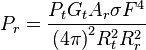
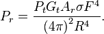
Oscillator frequency 
Intrinsic stand-off ratio h =0.4 to 0.6
h =0.5 (we take)
substituting the value of h in (1)

Capacitor C is charged through R towards supply voltage VBB. As long as capacitor voltage VE is below a stand-off voltage VP set by the voltage across B1-B2 and the transistor stand-off ratio h .
Sweep Amplitude = VP-VV
from design specification 
Design of R
At peak point emitter voltage VE=VP and current through R is given by
At valley point 
Design of Capacitor


Design of RB1 and RB2
At the point where the capacitor voltage is equal to VP assuming IE=0A, the network of fig 4 results. VP is the voltage required to turn on the UJT.
But the intrinsic stand-off ratio h is given by the equation
Also 
Substituting (a) and (b) in equation (10) we get
RB2 is chosen as a low value resistor. Let it be 100W .
Hence the above equation becomes
Procedure: -
EDWinXP -> Schematic Editor: The circuit diagram is drawn by loading components from the library.Wiring and proper net assignment has been made. The values are assigned for relevant components.
EDWinXP -> Mixed Mode Simulator: The circuit is preprocessed. The test points and waveform markers are placed at C, Rb1 and Rb2. The Transient Analysis parameters have been set. The Transient Analysis is executed and output observed in the Waveform Viewer.
Result:
The output waveform may be observed in the waveform viewer.

No comments:
Post a Comment